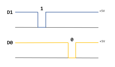
The Wiegand data wires D0 and D1.
Introduction
This article shows Wiegand protocol implementation on the Arduino Nano.
The Wiegand Protocol
The Wiegand protocol, albeit elementary, is still widely used by keyboards (and keycard readers) in access control systems. A brief description follows.
The Physical Layer
It is a very simple matter:
- There are
3 physical wires, namely D0, D1 and GROUND. - When there is no transmission, both
D0 and D1 are tied to +5V. - A logical
0 happens when D0 goes low (0V) while D1 remains high. On the other hand, a logical 1 happens when D1 goes low while D0 remains high (see the above picture). - Each data bit (either
0 or 1) must be followed by a pause interval. There are timing requirements for both data pulses and pause intervals (for details and references, please see the Wiegand Wikipedia page).
In my arrangement, the physical layer is represented by the Nano digital pins 2 (D0), 3 (D1) and GROUND. I use it to implement the 26-bit protocol.
The 26-bit Protocol
The Wiegand 'message' is just a 24-bit numeric code framed by two parity bits:
PXXXXXXXXXXXXXXXXXXXXXXXXQ
The heading parity bit P is added to the leftmost group of 12 bits (MSB) in order to obtain even parity. In a similar way, the trailing parity bit Q is added to the rightmost group in order to obtain odd parity.
For instance, assume the numeric code is 16777215, i.e., 0xFFFFFF (all ones):
P111111111111111111111111Q
In order to give even parity to the leftmost group of bits, we have to set P=0. On the other hand, in order to obtain odd parity in the rightmost one, we have to set Q=1.
Hence the final 26-bit code is:
01111111111111111111111111
Using the Sketch
Open the Serial Monitor tool: Arduino waits for a numeric code followed by a newline (see the picture below).

The Serial Monitor Tool
On successful reception of the numeric code, the corresponding Wiegand message is produced on digital pins 2, 3.
Some patterns captured by my trustworthy RIGOL scope:

The 16777215 (0xFFFFFF) code: yellow channel is Wiegand D0, blue channel is D1

The 0 code: note the last bit set to 1 in order to obtain trailing odd parity.

The 11184810 (0xAAAAAA) code flips all the bits.

This is a particular of the 0xAAAAAA pattern, showing the idle-to-data transition of the communication line.
Timings
In order to fulfill Wiegand timing constraints, the Arduino delayMicroseconds function is used. While results are not brilliant, protocols requirements are met.

Data pulse timing.

Interval pulse timing.
The Code
The code is simple and heavily commented. The workhorse functions are reported in the below snippets:
void outwiegbit(unsigned int b)
{
int sel = b == 0 ? W_D0 : W_D1;
digitalWrite(sel, 0);
delayMicroseconds(80);
digitalWrite(sel, 1);
delayMicroseconds(240);
}
The outwiegbit trivially outputs a bit on Wiegand outputs with proper timings:
void outwieg26(uint32_t u32)
{
uint32_t tmp = u32;
unsigned int p_even = 0;
unsigned int p_odd = 1;
for (int n=0; n<12; ++n)
{
p_odd ^= (tmp & 1);
tmp >>= 1;
}
for (int n=12; n<24; ++n)
{
p_even ^= (tmp & 1);
tmp >>= 1;
}
outwiegbit(p_even);
for (int n=0; n<24; ++n)
{
outwiegbit((u32 >> (23-n)) & 1);
}
outwiegbit(p_odd);
}
The outwieg26 outputs a 26-bit code. Heading (even) and trailing (odd) parity bits are first computed on the actual 24-bit code.
Points of Interest
Building a Wiegand code generator on Arduino was really quick.
Another step could be adding a keypad in order to create a real standalone control access device.
History
- 2nd July, 2018 - First revision
